MakerCamp
Research at Scale
By Yunyi Zhu

As a graduate student in digital fabrication, part of my research involves prototyping flexible PCBs in the lab with lasers/plotters/milling machines, and then ordering them from Shenzhen after finalizing the design. I was always stunned by the quality of the ones that we ended up ordering and became curious about the industry and the city behind it.
This January, I finally had the opportunity to spend one month in Shenzhen to participate in the Research at Scale + Scalable HCI program, where a group of us visited factories around the city. While I did want to scout for some high-resolution 365nm UV displays for my ongoing research project, I was mostly just curious what was out there.
PCB Manufacturing and Seeed Factory
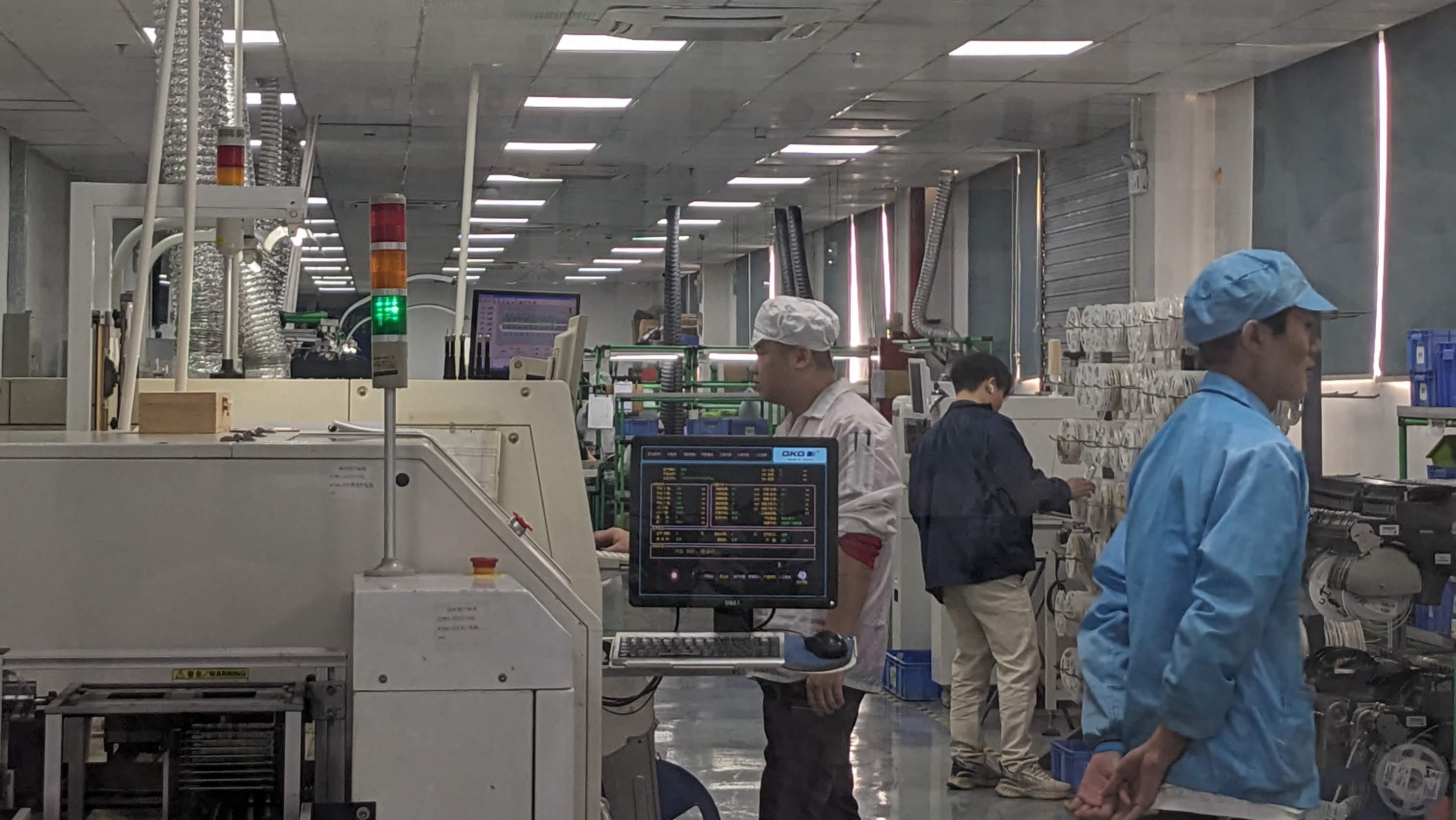 We visited Seeed Studio, who kindly sponsored our trip. Seeed develops prototype boards and showed us their factory, which is said to manufacture their own board prototypes at a quick turnaround cycle.
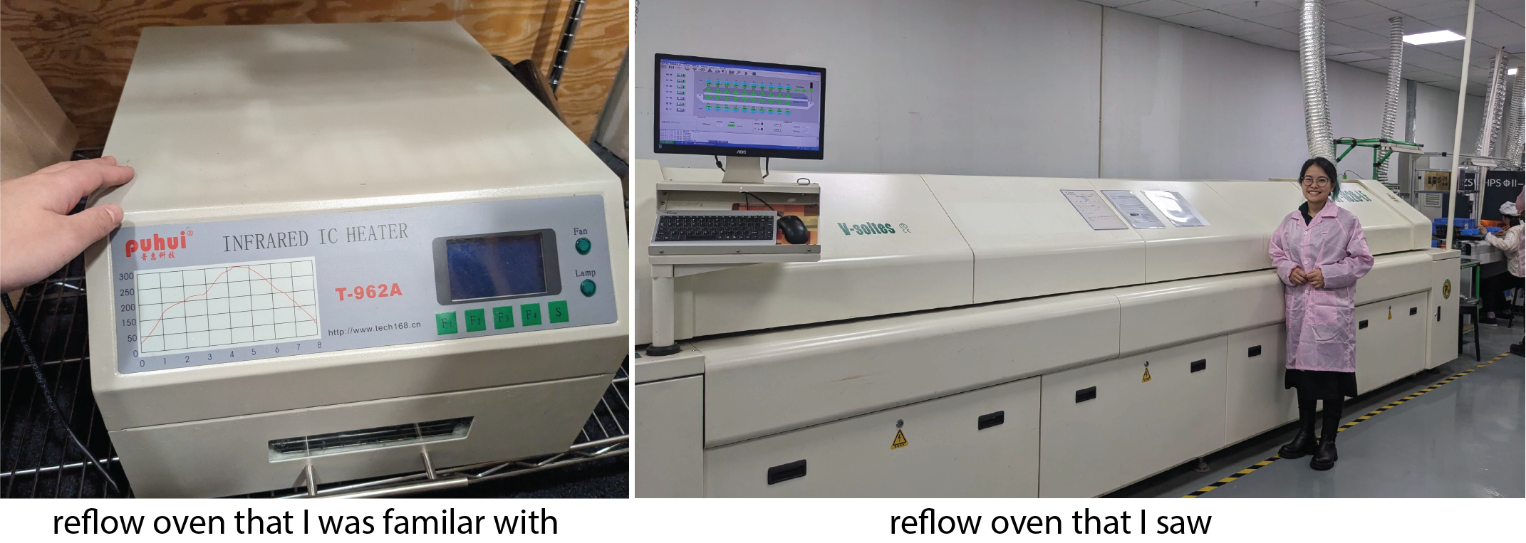
We saw cool pick-and-place machines, solder masks and machines that put solder paste onto the board, but what I liked the most was this industrial reflow oven, which is completely different from the reflow oven that I’m familiar with, and more similar to one in a cookie factory.
We also visited two more PCB companies, with one focusing on flexible PCBs. I was surprised that they also lasercut the trace patterns instead of etch them, probably because etching is soft banned in Shenzhen and the ones relying on etching moved outside the city.
I appreciate how much testing was involved in making one PCB. Just like what I was used to in the lab, people in the factories test all of the products and sometimes intermediate steps throughout the manufacturing process. This really makes me appreciate the boards that we used to buy with a click of a button.
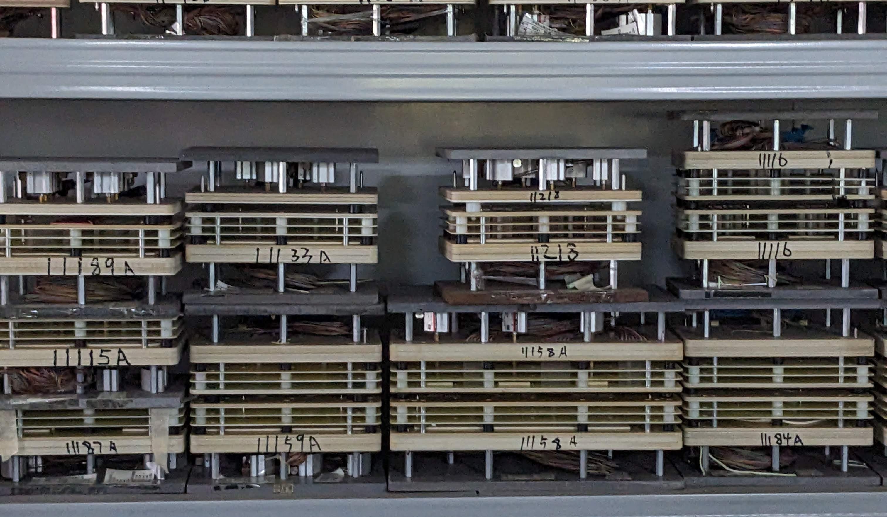 Testing jigs.
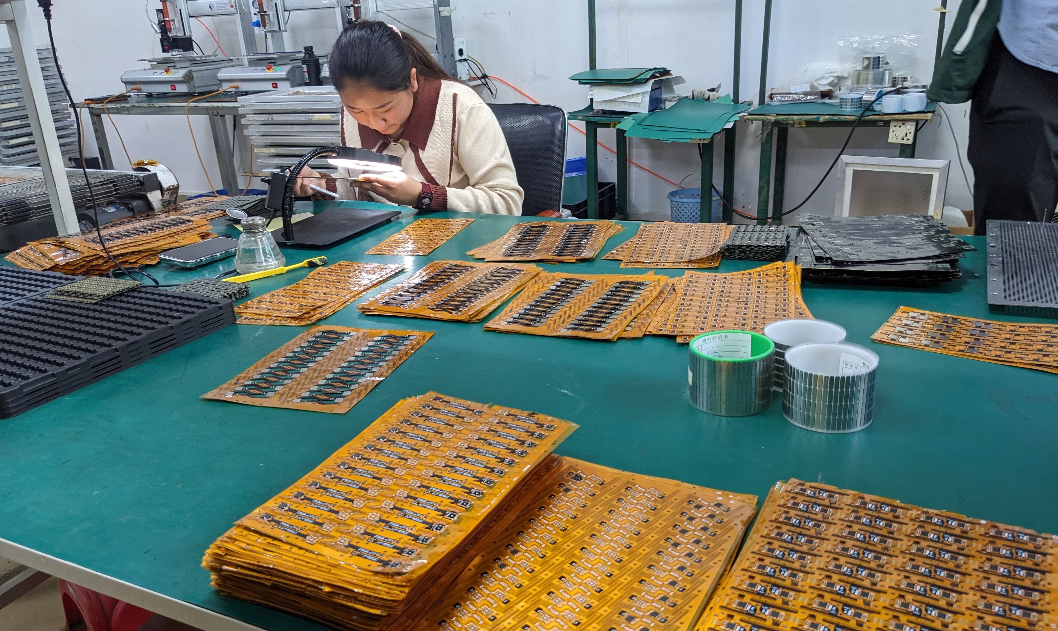 People in the factory visually inspect (look at) the PCBs and look for potential manufacture issues (photo permitted).
Display Factories
Closer to my research are the display companies, such as ones that make LCD or LED displays.
HiFly LCD Display
We visited HiFly LCD, an LCD display manufaturing company, which super openly showed us their assembly line, testing equipments… and even disassembled a display for us! Hila, Ganit and I ended up ordering some non-assembled LCDs from them for future testing.
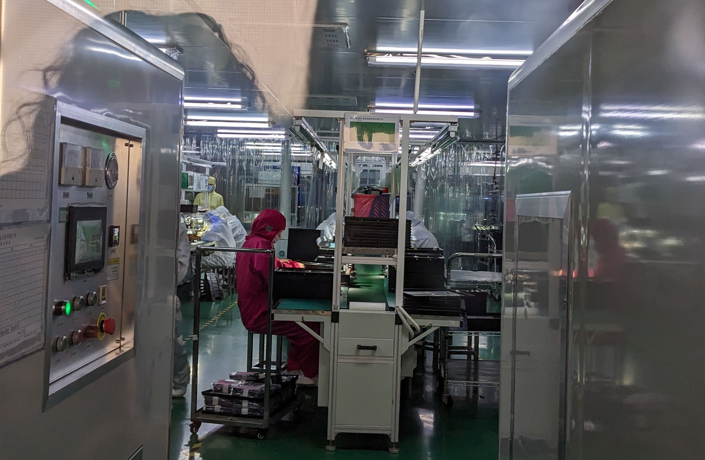 Manual assembly workers in the clean room, which is kept humid so that the particles drop to the ground quickly.
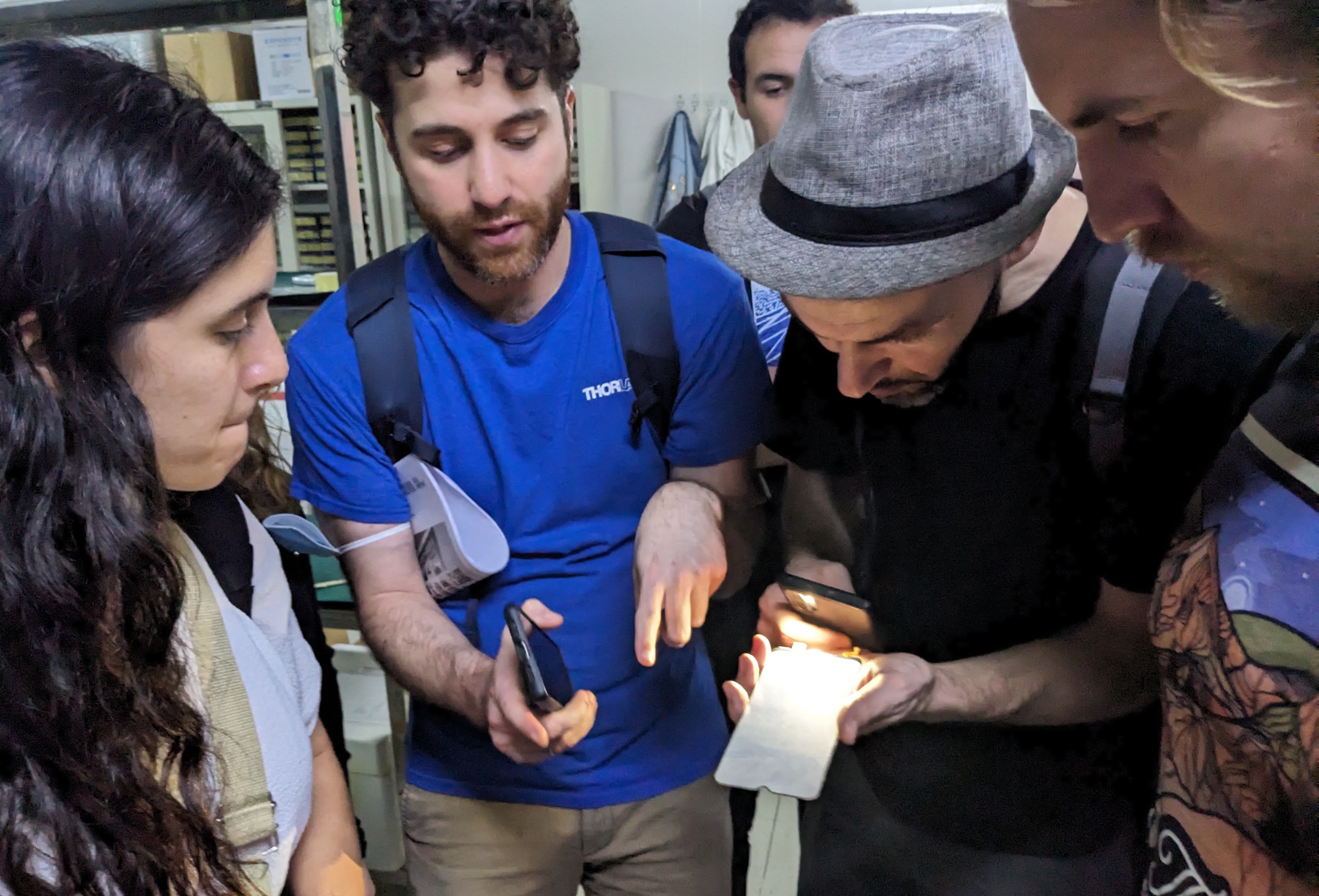 We were inspecting a backlight diffuser and looking for where the LEDs were mounted (they are on the side and super small).
UniLumin LED Display
We also visited Unilumin, a company that manufactures large scale and high resolution LED displays. We looked at their showroom and an expert kindly explained to us how everything worked and gave us some sample panels for free, which I have brought back to MIT.
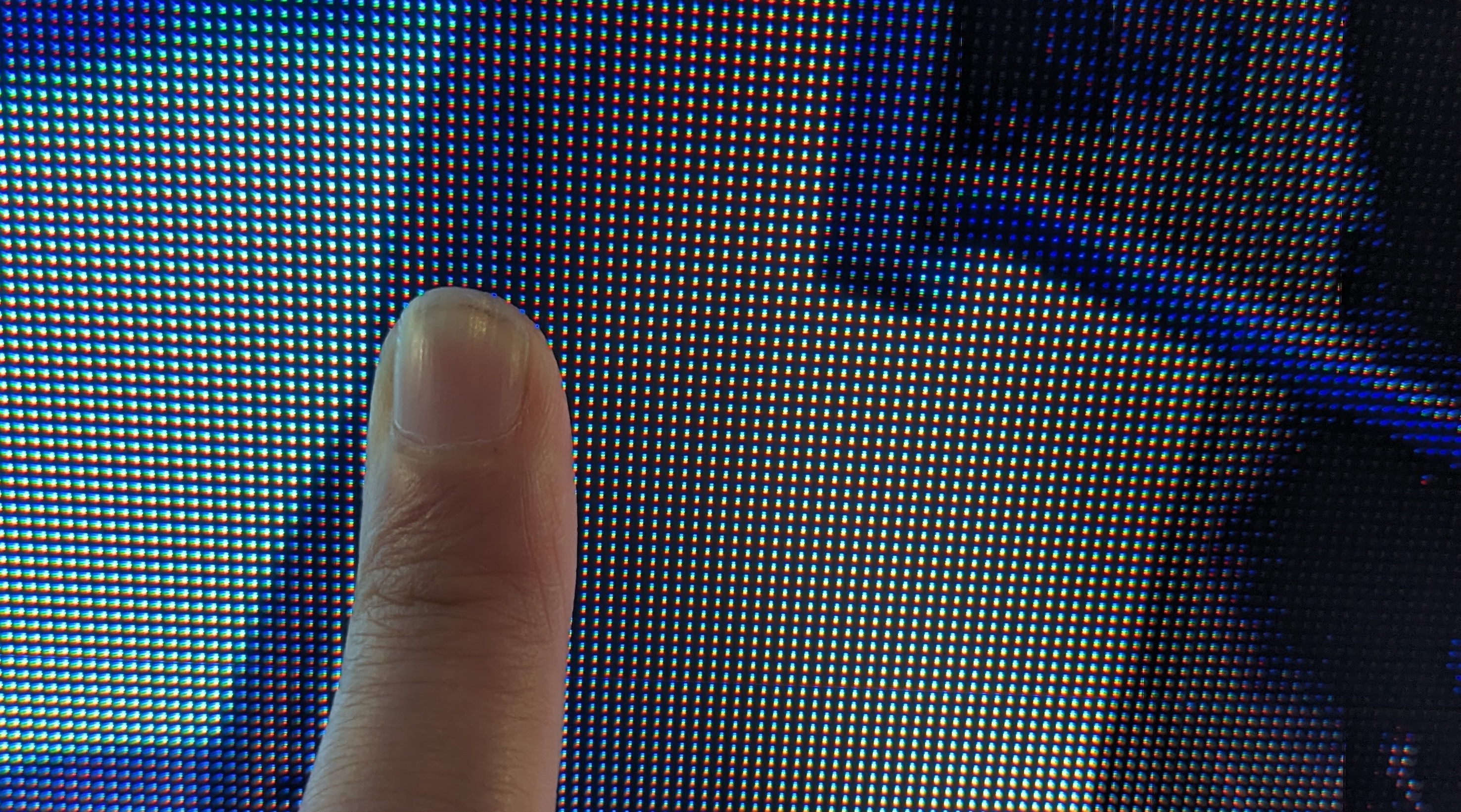 Super high resolution COB LED display, with pitch size of 0.4mm. (This is crazy!)
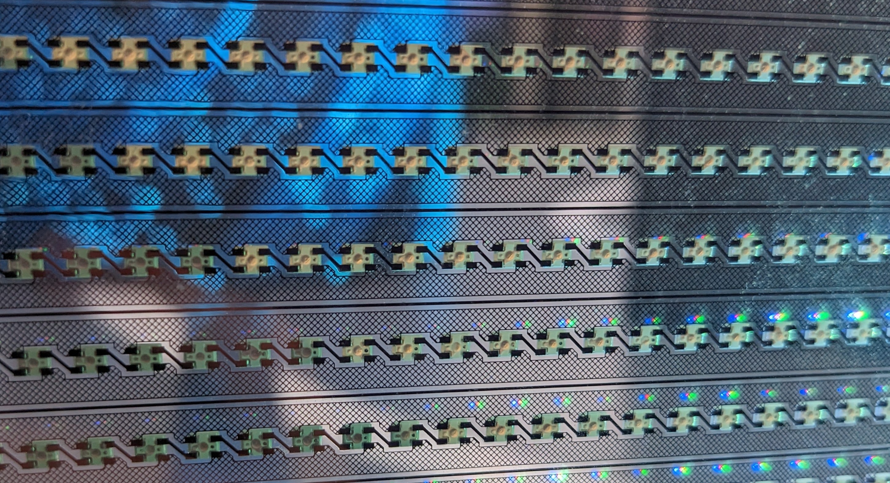 Transluscent addressable SMD LED array circuit (LED size 3.5mm, pitch size about 6mm). (Super beautiful!)
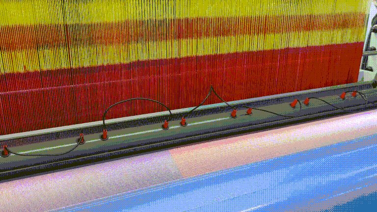
Textile Companies
K-Tech Knitting Company
We visited K-Tech, the knitting company that donated the Shimaseki in media lab. I’m surprised how open they are towards us about all of the machines, testing equipment, design processes and potential collaboration.
 Mesmerizing flat knitting machine.
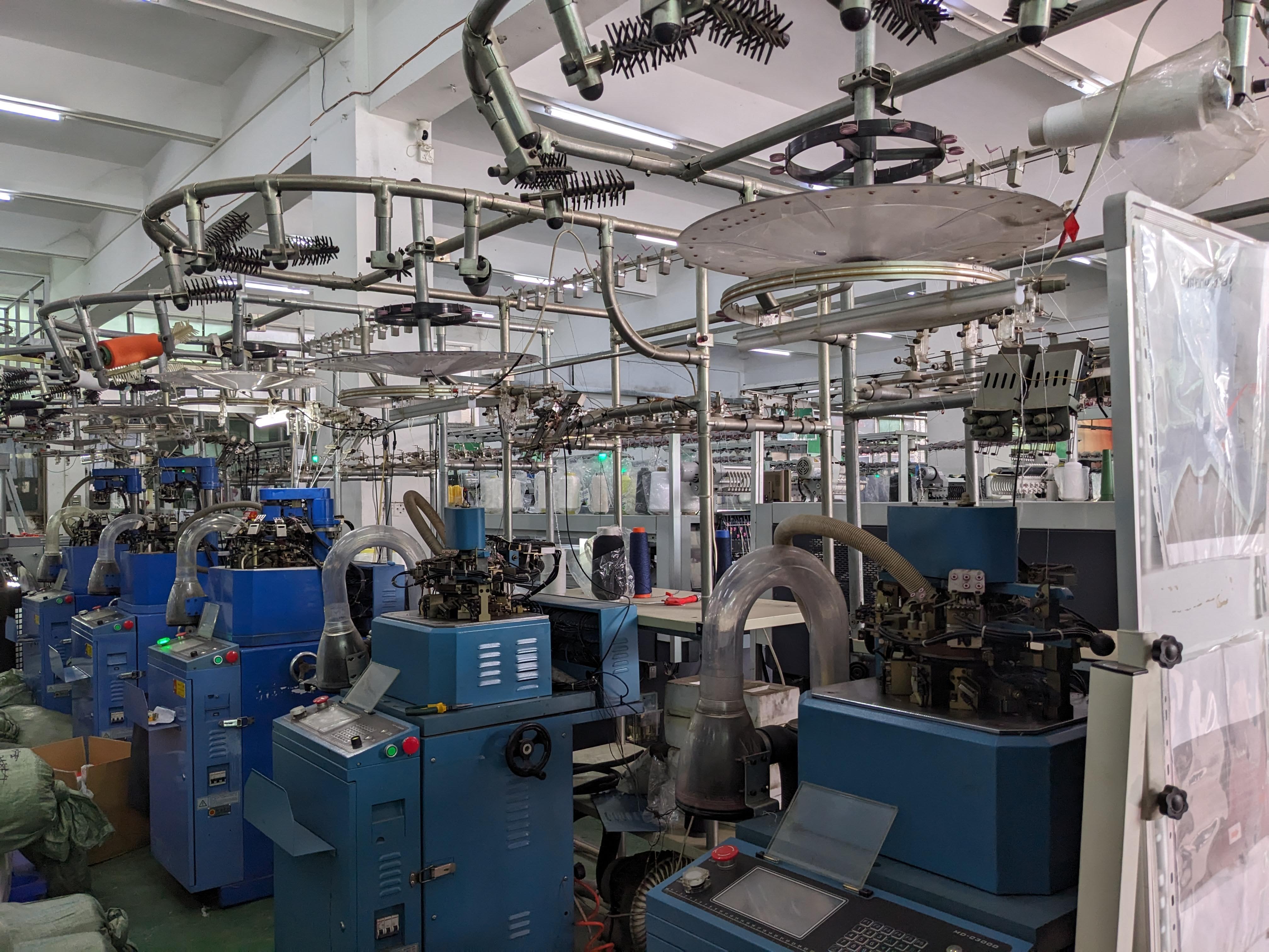 Rows of circular knitting machines.
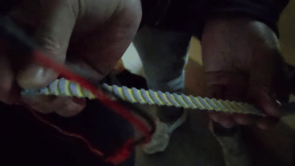
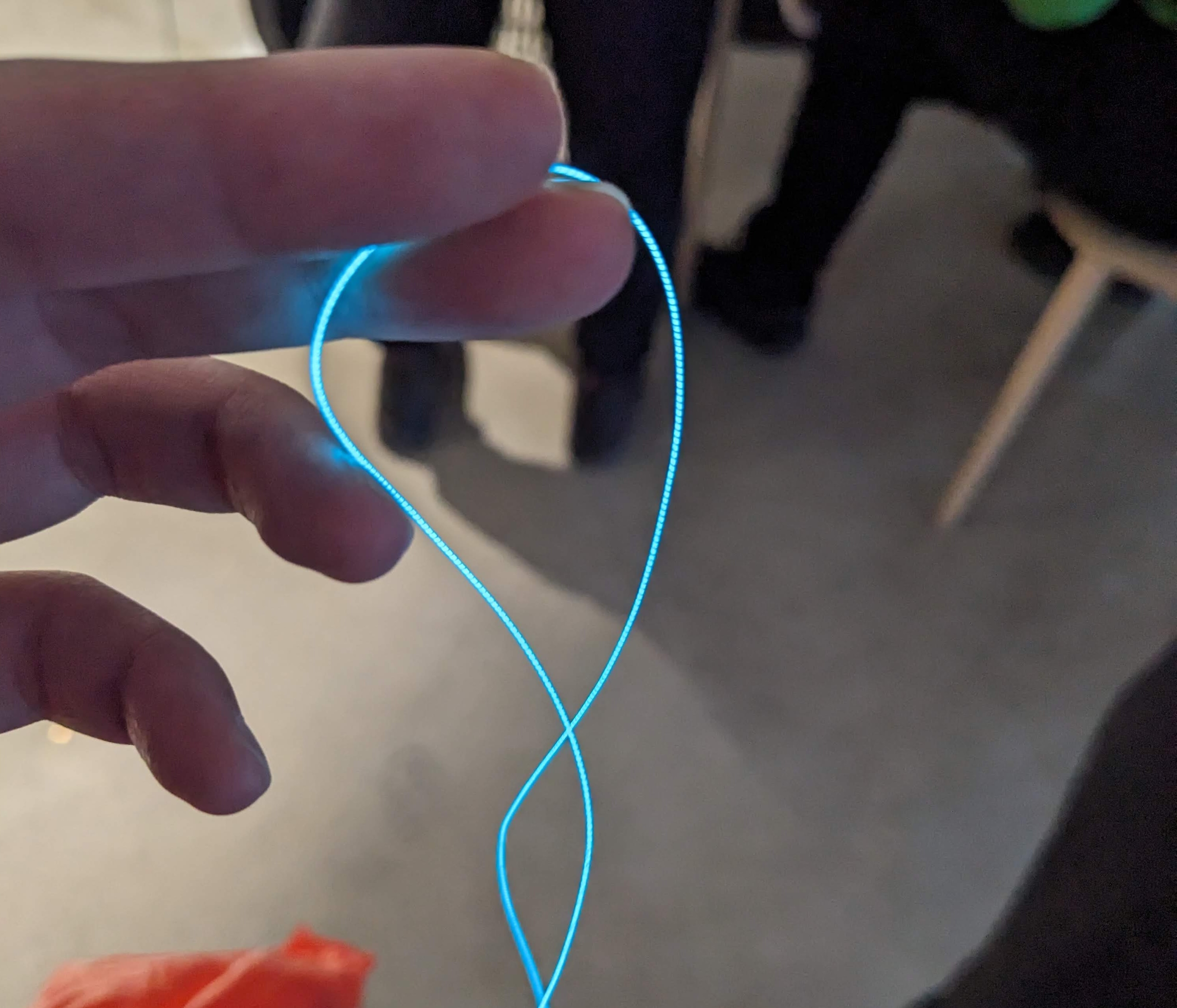
This is not optical fiber but electroluminscent yarns. The advantage is that they are much thinner and flexible, and thus can be knitted. If you knit an optical fiber, it will either break or leak some light.
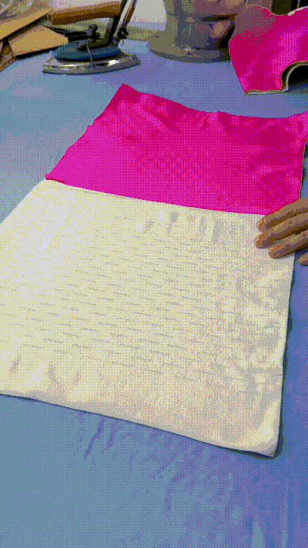
Andy showed us how to proprocess knitted bags with slits sealed with yarn that evaporate at high temperature. Ironing it creates the holes on the surface of the bag.
Electroluminescent Textile
Guangrun, a startup company that makes electroluminscent displays, also showed us their products in SUSTech.
 This EL fiber is super flexible and has relatively homogenous light intensity throughout the fiber.
Market Visits
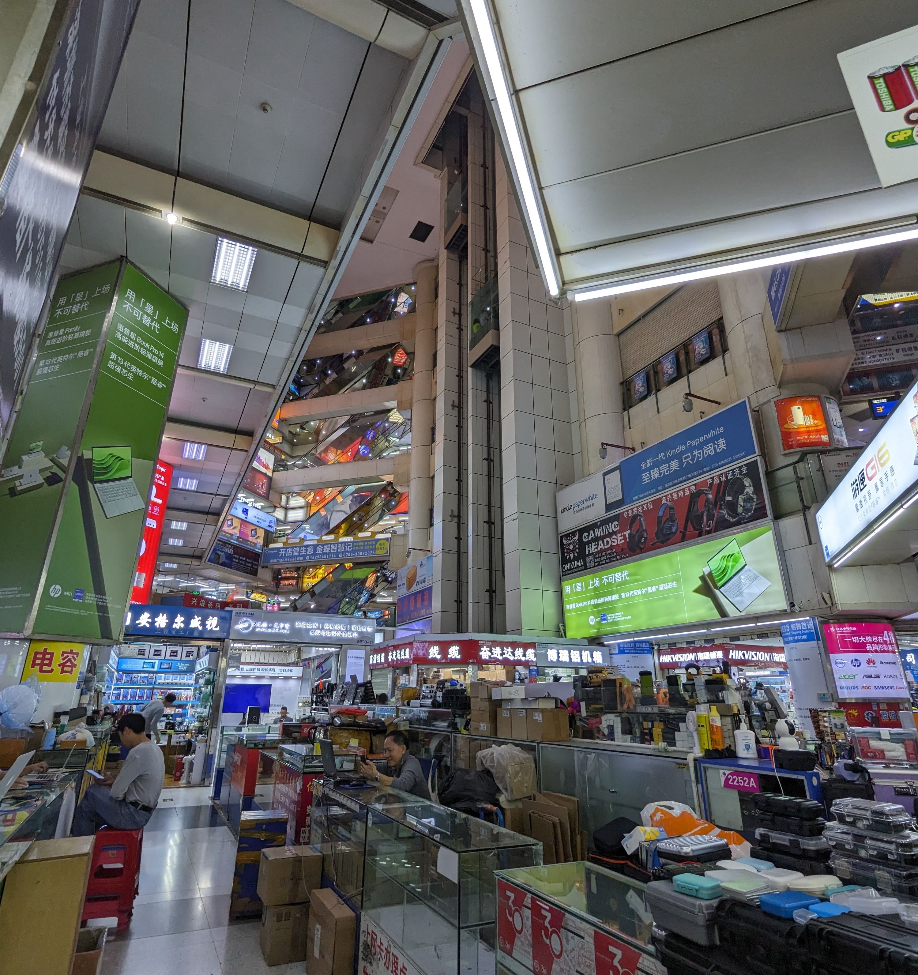
HuaQiangBei 华强北
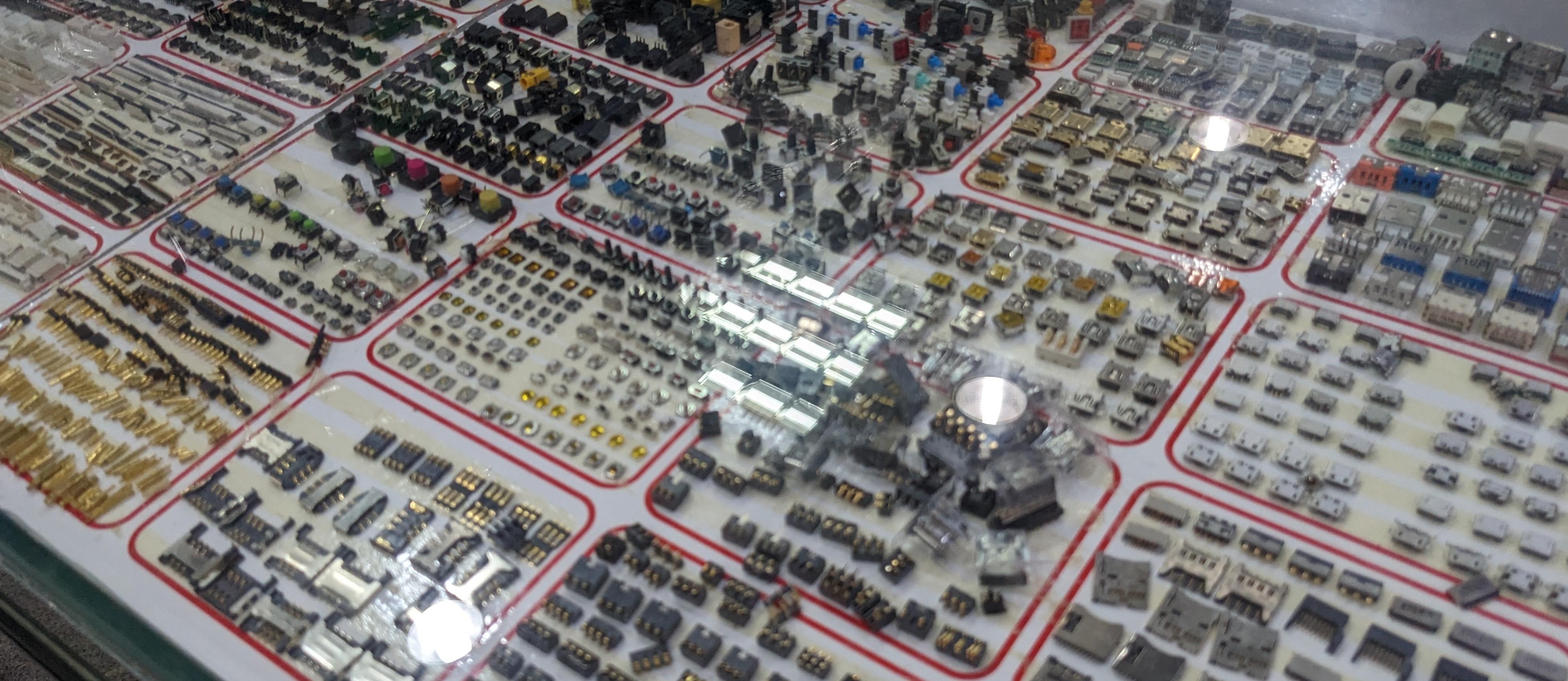
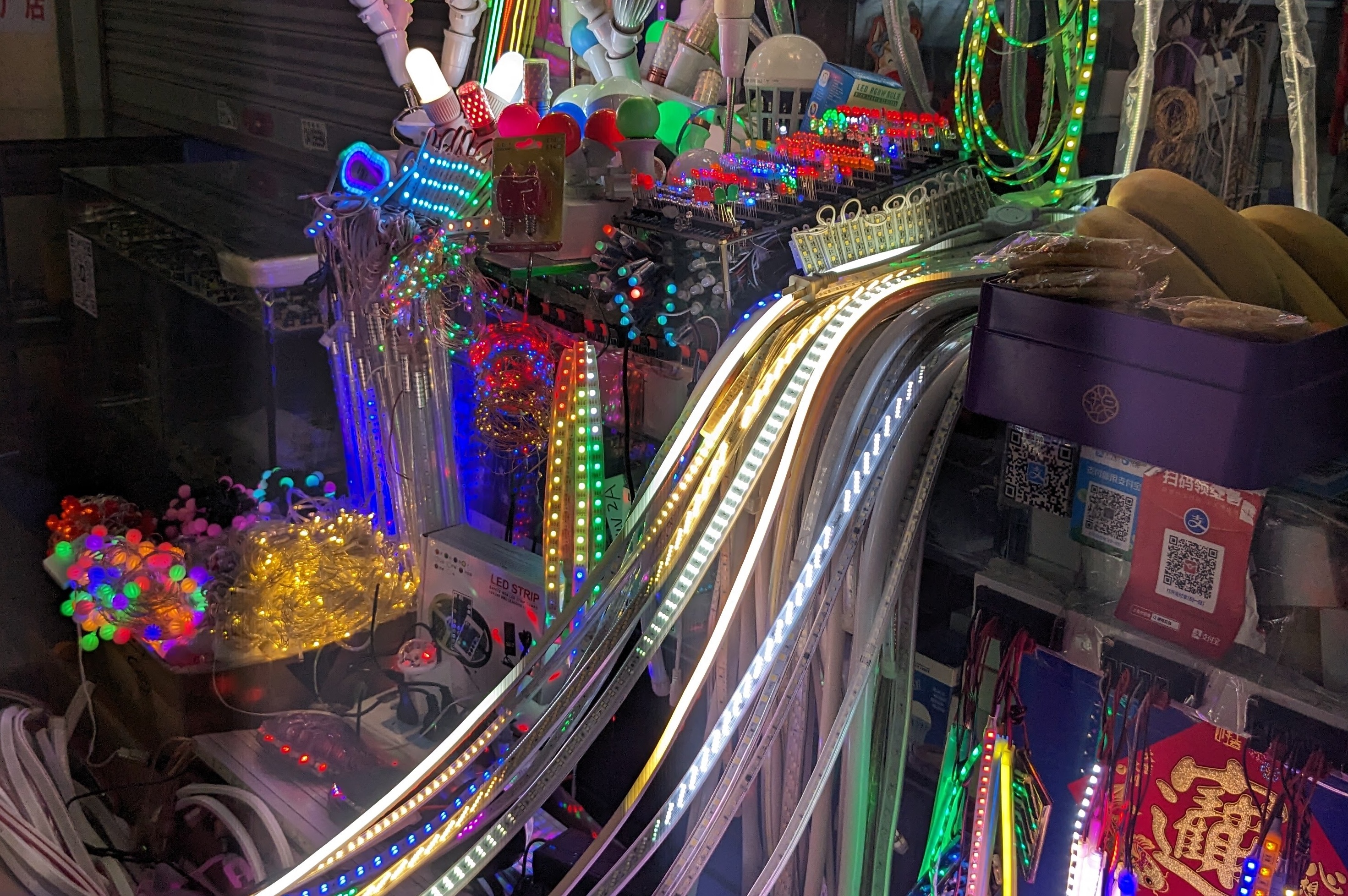
We were at Huaqiangbei! This massive neighborhood has everything. It’s a great place to explore, get samples, and chat with the sellers about both their products and their family (start with “how old is your child”).
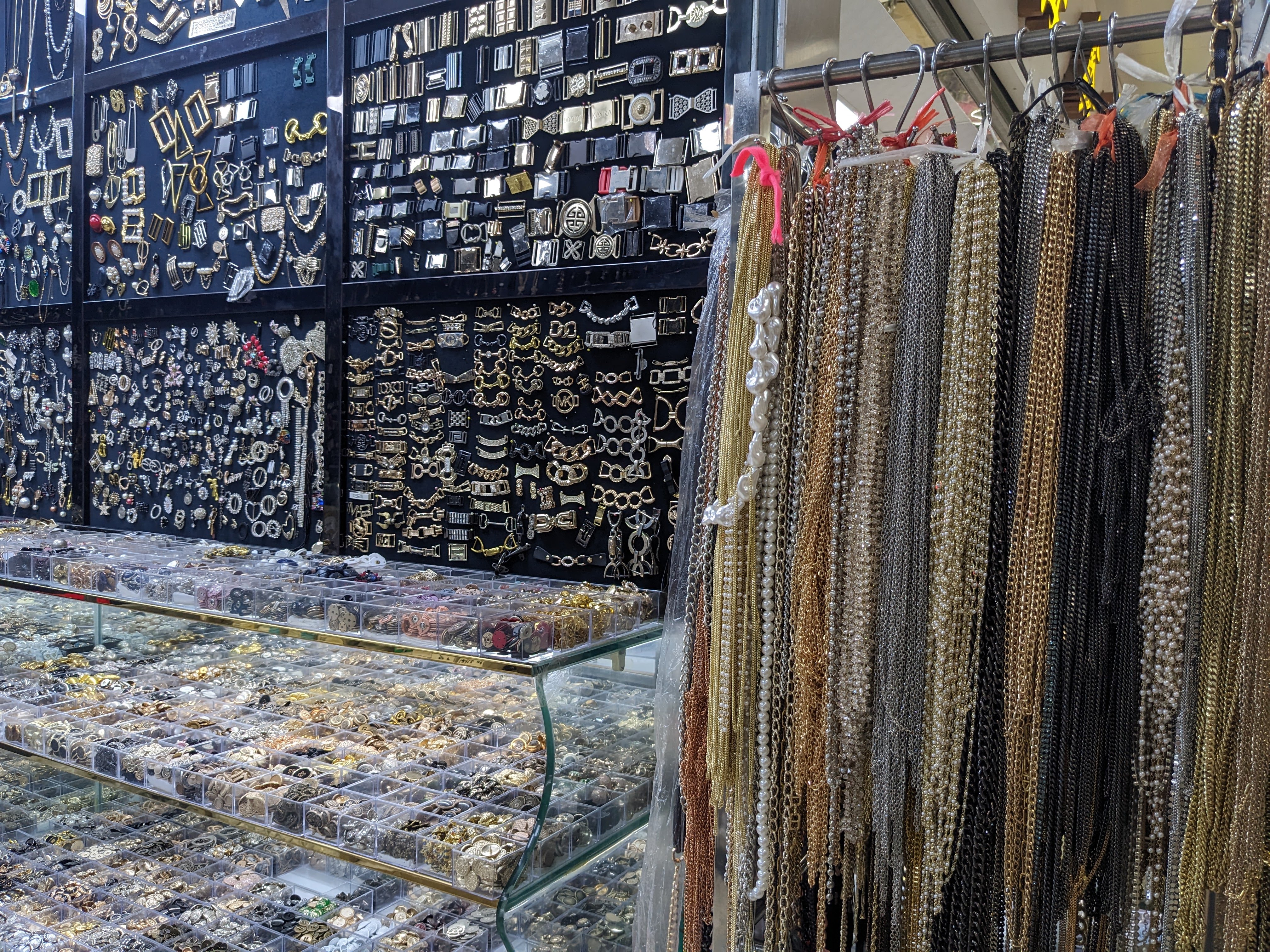
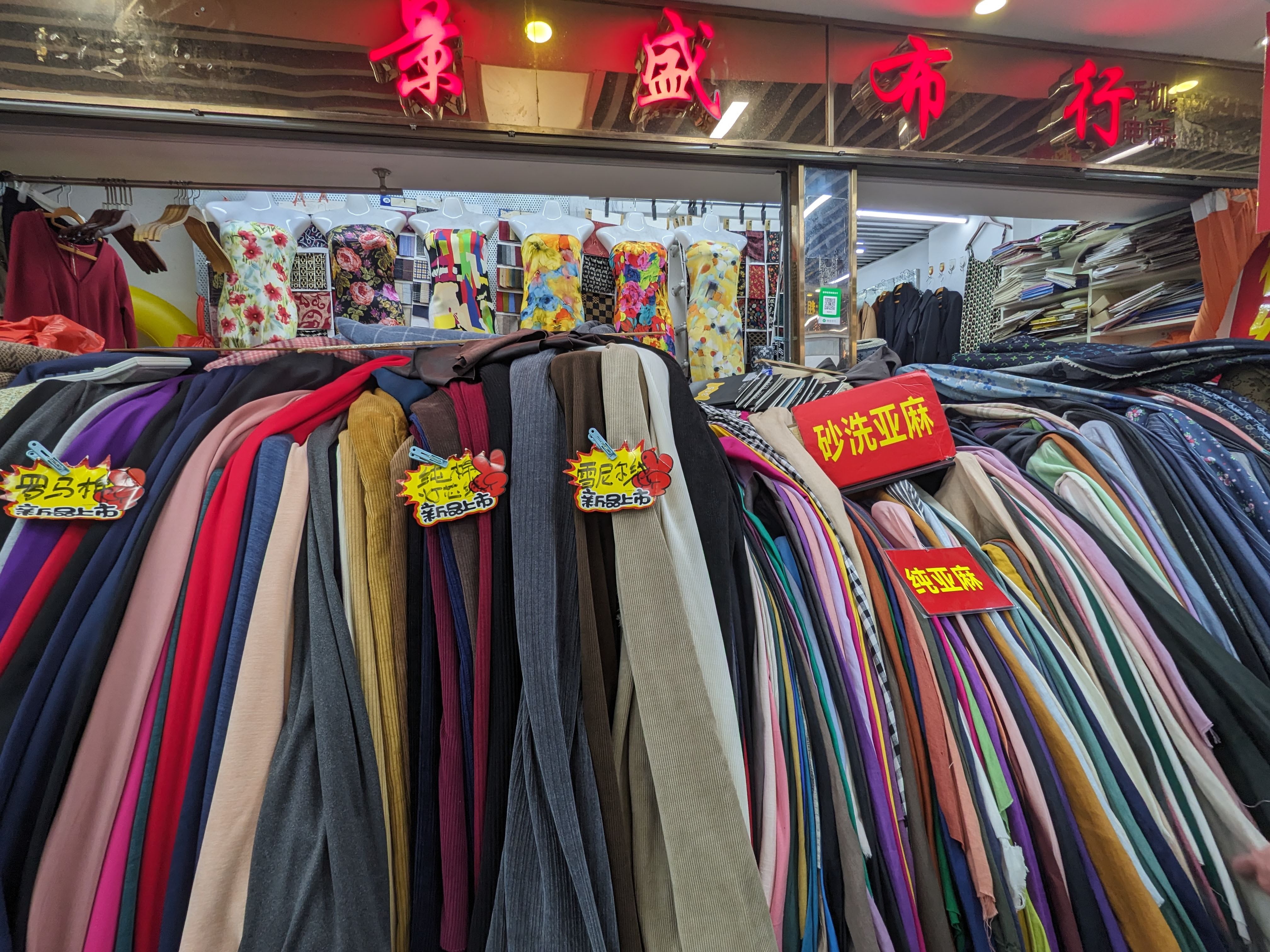
Textile Market
While I had heard that Guangzhou has the best textile market, the ones in Shenzhen were also amazing! It was nice feeling all those textile with your hand.
More about Shenzhen
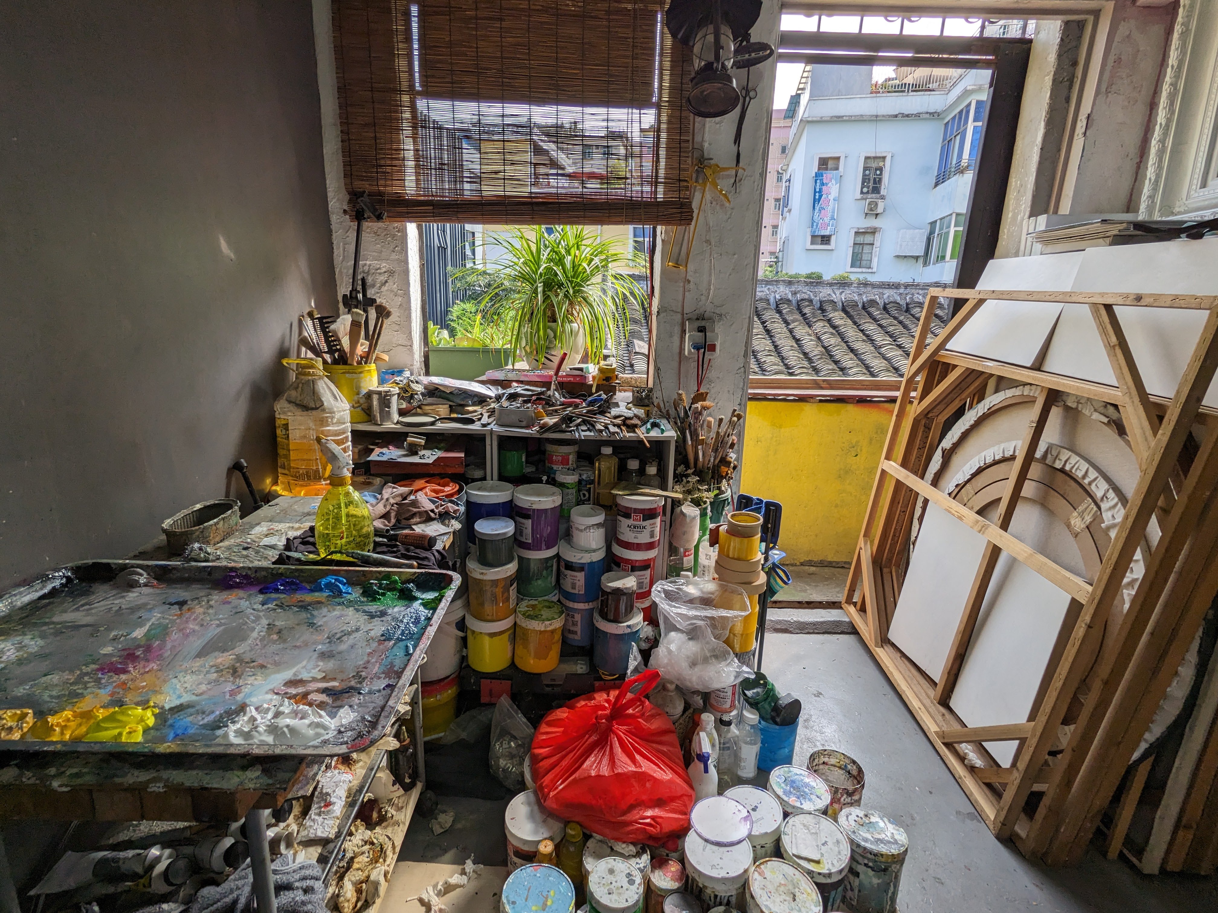
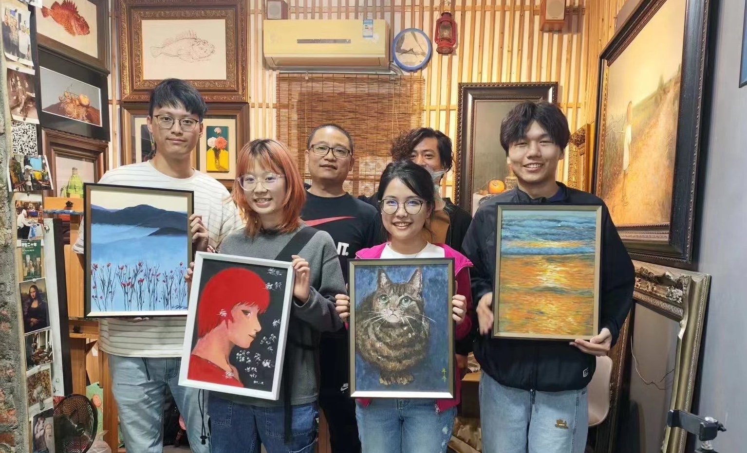
Dafen Oil Painting Village
We went to an artist’s studio in Dafen and learned oil painting.
Galleries
We also went to several art galleries.
Shenzhen is beautiful for its technology and its people. I enjoyed talking with the taxi drivers about their new year plans, trying unique street foods and bubble teas and unfortunately resolving payment issues for friends without a local phone number. This trip has left me with so many eye-opening moments and nice memories, and I look forward to checking back in a few years!
Yunyi Zhu - yunyizhu@mit.edu